The Basics of Charged Device Model
The semiconductor industry has created test models to determine the sensitivity of a packaged device to an electrostatic discharge (ESD). The first model to assess a device’s sensitivity to ESD events was the Human Body Model (HBM), which tested ESD events that occur when a charged person touches one pin while another is grounded. Modern automated semiconductor manufacturing techniques reduce human contact with device pins, resulting in rare instances of this type of damage.
What is the Charged Device Model?
A more important model characterizing ESD damage to semiconductors is Charged Device Model (CDM). Failure studies by device manufacturers have indicated that as much as 99% of device failures are due to CDM damage. After devices are mounted on circuit boards there are discharges like CDM, known as Charged Board Events (CBE). These events are of increasing importance to the contract manufacturers (CM) that assemble electronic systems.
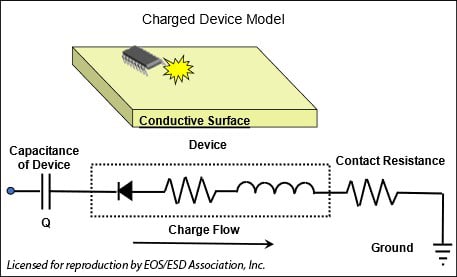
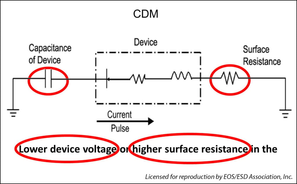
CDM results from charge on the device package, circuit board, or nearby object. The result of this charge is a voltage induced on the pins of the device. If the device pins contact a conductive surface under these conditions, an ESD event will occur. The magnitude of the ESD event will depend on the quantity of charge on the device package, circuit board, or nearby object, and the resistance in the discharge path. See Figure 1.
The problem is the resulting discharge current. To avoid the damage of the device’s internal circuitry, protection networks are integrated into the device or circuit board to redirect the discharge current to the ground.
Charged device model testers determine what level of CDM discharge causes device damage by placing the device package on a metal plate with the pins facing up. The voltage applied to the metal plate induces a corresponding voltage on the pins of the device. A current probe discharges each pin individually and can monitor the current in the ESD that results.
The voltage applied to the plate increases until it results in device damage and the last voltage applied without damage is referred to as the CDM damage threshold. Mounting a semiconductor device on a circuit board changes the ESD damage threshold. In addition to the charge on the package of the device, the charge on the circuit board and other components connected to the device must be considered. In many cases, CBE device damage occurs at lower voltages than the CDM damage threshold.
What are Charged Board Events?
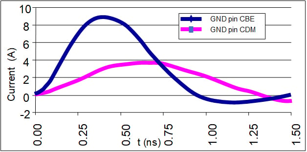
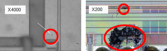
After mounting devices on circuit boards, there are discharges similar to CDM, known as Charged Board Events (CBE). Awareness of these events is increasingly important to contract manufacturers that assemble electronic systems. CBE causes greater damage than CDM and occurs at lower voltages due to increased capacitance. Figure 2 compares discharge currents from a semiconductor device after it has been mounted on a circuit board. Discharge currents are more than twice as high when mounted on a circuit board. Figure 3 shows the damage to the device caused by CDM discharge and CBE. The greater damage caused by CBE is often mistaken for electrical overstress (EOS). It is estimated that as many as 50% of failures designated as EOS are actually caused by CBE static discharges.
(Courtesy of Analog Devices and Dangelmayer Associates)
(Courtesy of Analog Devices and Dangelmayer Associates)
Charged Device Model Industry Standards
ANSI/ESD S20.20
Various industry standards identify CDM ESD as a problem and some propose acceptable CDM damage thresholds and CDM mitigation methods. One of the most important ESD control standards is ANSI/ESD S20.20 – ESD Association Standard for the Development of an Electrostatic Discharge Control Program for the Protection of Electrical and Electronic Parts, Assemblies, and Equipment.1
This document contains information for mitigating harm to devices with a damage threshold of 100 volts HBM and 200 volts CDM. The document provides comprehensive information for mitigating HBM discharges, but little information specific to the mitigation of CDM discharges. Fortunately, many of the HBM ESD control methods apply to prevent CDM discharges.
White Paper 2
White Paper 2 from the Industry Council on ESD Target Values is a more comprehensive document regarding the charged device model.2 This document provides an industry-wide analysis of ESD-damaged devices and concludes that CDM discharges are the major cause of device damage. While not an industry standard, it provides comprehensive information on the causes of CDM and recommends design rules for CDM immunity and mitigation methods for avoiding CDM discharges.
JEP-157A
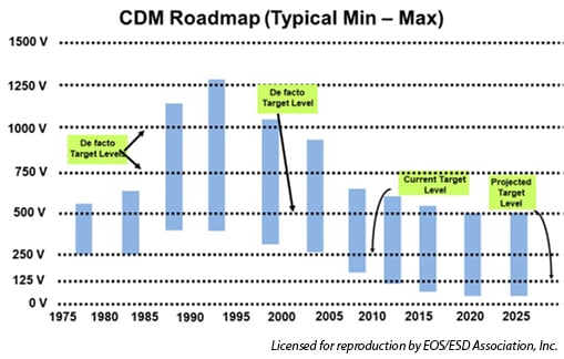
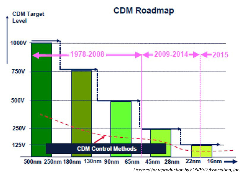
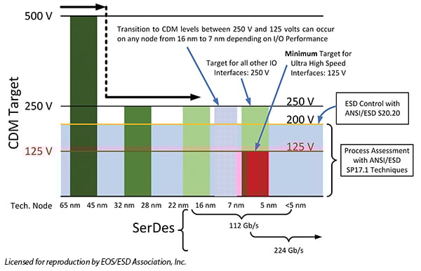
JEDEC, the semiconductor industry trade organization, released document JEP-157A – Recommended ESD-CDM Target Levels, containing much of the information from White Paper 2.3 This document recommends a CDM damage threshold of 250 volts for standard semiconductors and 125 volts for high-performance semiconductors. It points out that these limits will certainly become lower as semiconductor geometry continues to shrink. It also contains general methods for mitigating CDM damage. Figures 4, 5, and 6 illustrate industry roadmaps for CDM and CDM Mitigation.
Controlling CDM – Mitigation Methods
While industry documents do contain mitigation methods for CDM, they are not precisely spelled out. They do not provide a definitive plan to eradicate CDM discharges. For example, if we look at the basic CDM mitigation methods as shown in Figure 7, we can ask, “Which of these methodologies is encompassed within ANSI/ESD S20.20?”
ESD TR20.20-2022
The proposed solution involves solely the technique of voltage reduction on the device. But the latest version of S20.20 has removed the designation of air ionization as the preferred method of accomplishing this. For information on mitigation methods, one must have the companion document, ESD TR20.20-2022 – Handbook for the Development of an Electrostatic Discharge Control Program for the Protection of Electronic Parts, Assemblies, and Equipment.5 This document specifies air ionization as the method to lower device voltage. Refer to Figure 7.
Method 1
As shown above, the primary method of CDM Mitigation is lowering the device voltage by reducing the charge on the device (V = Q/C). Air ionization is used to neutralize the charge and reduce the charge on circuit boards, components connected to the device, and nearby charged objects. For residing charges on objects separated from the device, shielding can also be effective in preventing CDM discharges.
Method 2
The second method of CDM mitigation is rarely described by industry standards. This involves increasing the surface resistance at the point of contact between the device pins and the conductive surface.
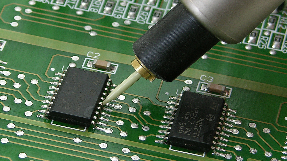
When establishing a CDM ESD control program, using static dissipative materials at the point of contact is the first mitigation method that should be applied. This is a passive method of ESD control, typically low cost, reliable, and requiring little or no maintenance. There are many materials , classified as static dissipative, that will increase surface resistance at the point of contact and eliminate damaging CDM discharges. Typically, the surface resistance at the point of contact should be greater than 104 ohms to prevent CDM ESD down to the 50-volt level and greater than 105 ohms at the 50-volt level and below.
In applications where it is necessary to mitigate the possibility of CDM ESD, use static dissipative materials at the point of contact and use air ionization to lower the voltage on the device pins. The use of ionization is particularly important to prevent ESD when the device pins must touch a conductive surface. Employing air ionizers to control CDM ESD requires specialized ionizer features.
Specialized Ionizer Features
First, ionizers for CDM control must have an appropriate offset voltage (balance). While some types of ionizers have an intrinsic zero balance, electronic ionizers may have a non-zero value for the offset voltage. Typically, for CDM control, the ionizer offset voltage should be between 20% and 50% of the most sensitive CDM ESD damage threshold. Most ionizers used in CDM control applications can maintain better than +/-20 volts of offset voltage. This makes them suitable for devices with damage thresholds greater than 100 volts.
For applications below 100 volts, ionizers are available with offset voltages in the 5–10 volt range, as well as ionizers in the 1-3 volt range for even more sensitive applications.
Ionizers used for CDM ESD control must have methods to assure that they can maintain their offset voltage performance, as well as alarms to indicate when the ionizer is operating outside of its specifications. Various feedback methods, using internal or external sensors, are used to assure that the ionizers are operating as expected over time.
To alert users when the ionizer can no longer maintain its desired performance, alarm indicators are typically integrated into the feedback control system. Note that even with feedback and alarm circuitry, all ionizers will still require periodic maintenance and, in some cases, calibration. The facility maintenance program must include ionizers used for CDM control.
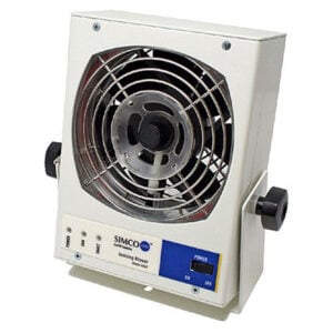
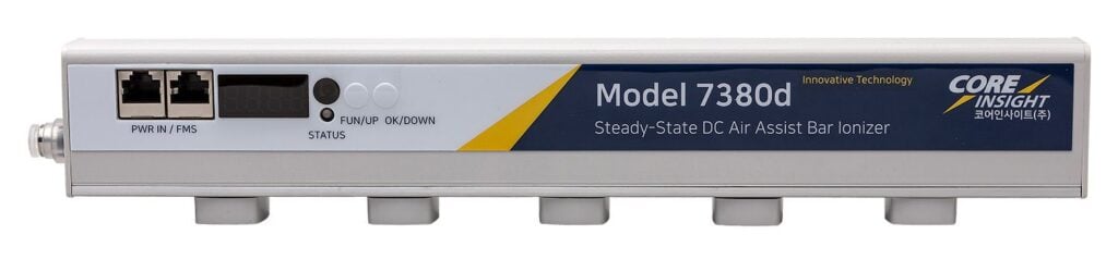
Ionizers for Charged Device Model Control
PAC’s lineup of ionizers, ionizing blowers, and bar ionizers are specifically designed to support your CDM ESD control program and protect your sensitive electronic devices with unparalleled precision.

References
[1] ANSI/ESD S20.20-2021, “Development of an Electrostatic Discharge Control Program for Protection of Electrical and Electronic Parts, Assemblies and Equipment”
[2] White Paper 2: A Case for Lowering Component Level CDM ESD Specifications and Requirements – May 2021, Rev 3.0
[3] JEP-157A – Recommended ESD-CDM Target Levels
[4] ESD Technology Roadmap from the ESD Association
[5] ESD TR20.20 – Handbook for the Development of an Electrostatic Discharge Control Program for the Protection of Electronic Parts, Assemblies, and Equipment, currently being revised.